Immersion Lithography Technology
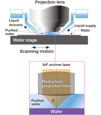
Immersion lithography is a technology in which lithographic exposure is applied to a resist-coated wafer via purified water that is introduced between the projection lens of a semiconductor exposure system (scanner) and the wafer. Previously, leading-edge scanners in IC mass-production lines used ArF*1 193nm*2 excimer lasers as their light source, and ordinary projection lenses (not the immersion type). At that time, their resolution limit was said to be in the order of 65nm. The idea behind immersion lithography is to use a light source of the same wavelength and yet realize a semiconductor process at precision as high as 40-45nm.
The shorter the wavelength of the light source and the higher the numerical aperture of the projection lens, the higher the resolution of a semiconductor exposure system will be.
Its resolution is described by:
Resolution = k (process factor) x λ (wavelength of the illumination light)/NA
where NA is the numerical aperture of the lens, NA = n x sinθ, where n is the refractive index of the medium between the projection lens and the wafer, through which the exposure light passes.
Immersion Lithography Results
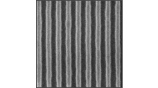
39 nm line-and-space pattern (NSR-S610C Topcoat-less Resist Imaging)
Previously, the medium was air, hence n = 1.0. θ represents the maximum incident angle formed by the exposure light with the normal to the wafer surface. If the refractive index is 1.0, theoretically NA is less than 1.0 at most, and realistically, it is no higher than 0.9 or so (θ = 65°).
In immersion lithography, the medium through which the exposure light passes has been changed to purified water (refractive index 1.44) instead of air. Therefore, the NA can be theoretically increased up to 1.44 times.
Nikon was the world’s first to develop an ArF immersion scanner for production — the NSR-S609B — a feat that broke the barrier of NA1.0 and reached NA1.07, enabling the mass production of 55nm devices, hitherto impossible with conventional ArF scanners. The NSR-S610C with NA1.30 realizes ultra-precision 40-45nm semiconductor processes. Both models are playing a vital role in the manufacturing frontlines of top-notch IC devices.
Immersion lithography technology enables IC microfabrication while minimizing changes in the IC manufacturing process that accompany the change of the laser wavelength — an achievement that was hardly possible with conventional technologies.
There were, however, a few issues that needed to be addressed in order for immersion lithography to materialize.
One issue was how to deal with the purified water filling the space between the projection lens and the wafer. The wafer stage starts and stops abruptly between every exposure. How to retain the water between the projection lens and the wafer was a problem that had to be solved. Furthermore, if vaporization heat is generated when purified water evaporates, water temperature drops, causing deviation in exposure accuracy. In addition, water marks caused by the evaporation of drops of water lead to pattern defects.
Believing the successful control of purified water to be a vital issue for immersion scanners to perform well on IC mass production lines without negatively affecting productivity, Nikon engineers concentrated on the development of this technology. The results were two new proprietary technologies. One, the Local Fill Nozzle, enables high-speed stage movement while reducing evaporation of purified water and the accompanying generation of vaporization heat that results in defective wafers. The other, the Tandem Stage, comprises two stages that individually perform exposure and calibration, thereby obviating the need to stop the supply of purified water during wafer exchange. This has enabled the Nikon immersion scanner to achieve both high productivity and high precision over long periods of time.
Immersion lithography that significantly extends the lifetime of ArF scanners plays a vital role in the frontlines of leading-edge devices.
- *1With a wavelength of 193nm, this type of laser is named after the inert gases used for discharge excitation: a mixture of argon (Ar) and fluorine (F) halogen.
- *2One billionth of a meter (10-9 meters).
Renewed March 2008
- News Release "Development of ArF Immersion Stepper for Mass-Production Applications" (February 19, 2004)
- News Release "Announcing the Sale of Nikon ArF Immersion Scanner NSR-S610C" (July 6, 2006)
- News Release "Nikon Completes Shipment of Immersion Scanners to All Major Semiconductor Manufacturing Regions of the World" (November 29, 2007)