Low-Reflectance Si Light Shielding Film Technology
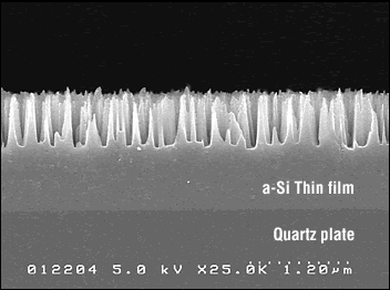
Fig. 1: Light shielding film cross-section structure
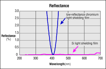
Fig. 2
Fig. 3
For optical systems, such as microscopes and various measuring devices, how to reduce stray light and flare that have negative impacts on observation and measurement is important. A generally used chromium light shielding film forms an antireflection film of chromic oxide on its surface, and reduces reflected light from a surface of the film. However, there were some problems in such method. For example, the reduction of reflectance is only effective with a certain wavelength area, and antireflection effect decreases depending on incidence angles of light.
Forming micro needle structure on single-crystal silicon (Si) surface is already known technology to absorb light and reduce reflectance ratio. Nikon applied a thin film technology and lithography to it. By forming micro needle structure on thin film Si surface, it becomes possible to manufacture a transmissive optical element that has a low reflecting light shielding film.
Fig. 1 shows a SEM picture of a cross section of "Low-Reflectance Si light shielding film".
"Low-Reflectance Si light shielding film" that Nikon developed first in the world has three features. Firstly, it has very low wavelength dependency. Fig. 2 shows wavelength dependence of reflectance for both low-Reflectance Si light shielding film and that for a Low-Reflectance chromium light shielding film. Low-Reflectance chromium light shielding film is effective for some certain wavelength areas which depend on thickness of a chromic oxide film (about 410nm*1 in the case of Fig. 2), but the antireflection performance is significantly less effective for other wavelength areas. On the other hand, low-Reflectance Si light shielding film realized reflectance of less than 0.1% in a wide wavelength area from 200nm to 620nm. Secondly, it is possible to form any shape of permeable aperture patterns at any position up to a several micrometer*2 sizes by using application of lithography technology. Furthermore, the less incidence angle dependence is one of the major characteristics.
Fig. 3 explains a principle why the needle structure formed on thin film Si surface can reduce reflectance. Some parts of the light reached on the needles are absorbed and changed to thermal energy. The light not absorbed on the surface of needles is reflected and some of the reflected light is absorbed by other needles and changed to thermal energy. Such process repeats and realizes reflectance of less than 0.1%. However, there are some other explanations about this principle apart from that explained in Fig. 3, and it is not yet investigated.
Low-Reflectance Si light shielding film that Nikon developed has excellent antireflection characteristics. It is also usable as a light shielding film of permeable optical elements. We can expect to use low-Reflectance Si light shielding film for microscopes or optical measuring devices that require confocal optical systems. Also, it may be applied to other optical systems and equipment widely.
- *1One billionth of a meter (10-9 meters).
- *2One millionth of a meter
Posted May 2006