Auto Macro Inspection Technology
In semiconductor device manufacturing, dozens of fine pattern layers are exposed onto a wafer by exposure tools such as a scanner. Those patterns are then inspected after each set of exposure and development to ensure the patterns are formed with the required design accuracy. One of the test equipment used for this inspection is the Nikon Auto Macro Inspection System (hereafter, called AMI). Although manual inspection used to be the main stream for macro inspection, the introduction of the AMI has enabled fully automatic macro inspection with high precision.
AMI overview
The macro inspection tool, AMI, doesn’t need to be equipped with high magnification optics simply because it is not a tool for individual pattern inspection. On the contrary, the AMI captures the image of the entire 300mm wafer with one shot in order to detect critical defects with a high rate of throughput.
On the AMI, specifically selected light illuminates the wafer surface and the reflected light is then analyzed as a captured image to detect defects. In the case where the repeated patterns on the wafer are uniform, the reflected light produces an image of uniform brightness. On the other hand, areas on the wafer that exhibit brightness levels different from the rest of the wafer indicate that those areas of pattern are defective.
Fig. 1: AMI optical system
The AMI targets the following main types of defects: defocus, resist coating errors, particles, and scratches on the wafer surface. One type of defocus defect is caused by scanner focus error, which results in a rectangular dark area because the focus shift occurs on one shot. The other defocus type, caused by a backside particle, swells up the region slightly and shows an image of a small, dark, donut-shaped area. The swollen region is the cause of this focus shift. Nikon has developed a defect detection technology that can distinguish between manufacturing fluctuations that are within spec and true defects. In the inspection process, the images of the inspected wafers are analyzed and compared to learned and stored information of normal manufactured wafers.
Scatter light optics and diffraction light optics
The AMI employs two distinct optical systems for defect detection. One system is scatter light optics. This method illuminates a wafer using a shallow light angle. The resultant scattered light caused by particles or scratches is then captured with a camera located above the wafer. Detecting this scattered light is similar to watching a star in the dark sky. Relatively small particles can be detected compared with the camera pixel size.
The other optical system utilizes reflected light and/or diffraction light. To capture the reflection image, this method illuminates a wafer on a tilted wafer chuck in order to make the incident light angle and the reflection light angle equal. This reflection light is effective for detecting coating errors. Diffraction light, on the other hand, is emitted from repeated patterns. Reflected light from one line pattern and a neighboring line pattern is intensified by interference. The intensified light emits to a particular angle related to the pattern pitch. The diffraction light emitting angle changes depending on the pattern pitch. The tilting angle of the wafer chuck is adjusted to match the pattern pitch of the wafer being inspected. Since the diffraction light intensity changes as the pattern shape changes, this diffraction image is effective for detecting defocus defect.
Without the need for high magnification optics, the AMI can detect the slight variations in shape of fine patterns via brightness changes of the captured images. In other words, the AMI can detect micro defects, defects of fine patterns, with its macro eyes: low magnification optics.
PER optics
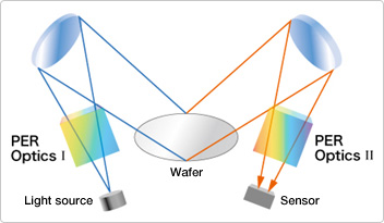
Fig. 2: Configuration of PER optical system
Even as the design rules of semiconductor devices continue to shrink year after year, wafer inspection using diffraction light continues to be an effective method of inspecting fine device patterns. However, the light source wavelength needs to be shorter and shorter as the pattern pitch gets finer and finer. A light source of 248nm, which is the shortest wavelength of the current AMI system, can inspect patterns with a half pitch of 70nm. To inspect a finer pattern of half pitch 55nm with diffraction light, a light source of 190nm wavelength would be required. Diffraction light will not be acquired from these fine pitch patterns if a light source with a longer wavelength is used. Manual macro inspection using a visual light source can be used for defocus detection as color variation. However, as the half pitch of the pattern becomes 70nm or less, these color variations also cannot be observed due to the same reason that the diffraction light doesn’t come out.
It could be possible to inspect half pitch 55nm wafers on the AMI using diffraction light if the equipped light source had a 190nm wavelength. However, such a system would be large and expensive. Moreover, this trend will continue as the pattern becomes finer and IC generations change.
Nikon has developed a new concept optical system as the answer to shrinking pattern design rules’ called PER, which stands for Pattern Edge Roughness optics. This optical system employs polarized light technology. The polarized light oscillates only in a particular direction. If the incident light on the wafer is polarized light, reflection light polarization status changes depending on the pattern condition. If the patterns are uniform, the polarization status changes likewise. If however some pattern area condition is different from the other areas, the change of polarization status is not uniform. This means the area will look different from the other areas on the wafer image, and thus be detected as a defect. Inspection with Nikon PER optics can keep pace with the technological innovation of semiconductor devices for half pitch of 55nm, 40nm or beyond without requiring a modification of the system for a shorter wavelength light source.
TLEX optics
In general, the topmost layer of pattern on a wafer is the inspection target. However, during inspection the lower layer signal is also inadvertently captured. This is a big issue for macro inspection. This is particularly an issue for patterns known as “via” which are used to connect wirings, or “damascene” patterns which are used for copper wirings. In these cases, the inspection target layer is the top resist layer, which is a translucent film, with metal wiring patterns below it. During inspection a very strong signal reflects from the lower layer of metal wirings, subsequently wiping out the signal from the top layer. Sophisticated technology is required to suppress this signal from the lower layer.
Fig. 3: Diffraction + TLEX principle
Nikon has developed TLEX optics; the abbreviation for Top Layer signal EXtraction. These optics are a combination of polarization technology and diffraction light optics. The diffracted signal from patterns with certain target pitch is selectively captured, and then only the signal from the top layer is extracted with polarization technology, which may contain defect information. In short, the TLEX optics removes the signal from the lower layer utilizing polarization technology.
AMI functions
One of the functions of the AMI is to discriminate between well-patterned wafers and defective ones, thus providing a pass or fail wafer evaluation. When defects are found, it is possible to reprocess the wafers by removing their resist in order to rescue the expensive wafers. The other important AMI function is to provide a warning of other processing equipment problems based on stored defect information within its database. For example, frequent defocus might indicate an exposure tool problem, and increasing resist coating errors could indicate something wrong with the coating equipment. A large amount of wafer loss can be prevented by quick readjustment of the equipment causing the problem. From this standpoint, an inspection of all the wafers is recommended versus a limited sampling plan. Inspecting all the wafers could send an early warning even for sudden serious process problems.
The latest Nikon AMI model has achieved a high throughput rate of 160 wafers per hour. Thus, the AMI makes it possible to inspect all 300mm wafers in production. In the field of semiconductor device manufacturing, the AMI is making significant contributions to increased yield as key equipment rather than a simple inspection tool.
Posted January 2008