High-Precision Thinfilms
Nikon multi-layer thinfilms, created using extremely smooth, flat films and precise thickness control, provide the precision and performance needed for use in such harsh environments as space systems. We have steadily perfected our technology to meet these requirements.
Today, Nikon devices utilizing high-precision thinfilms are applied to new products such as gain-flattening filters, key components in increasingly important optical communications, and substrateless filters.
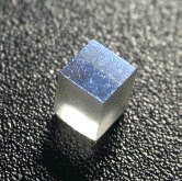
A multilayer filter measuring only 1.4mm on each side
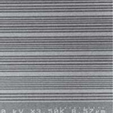
Photomicrograph of a cross-section of a multilayer film filter (3500x)
Optical thinfilm filters utilize the interference effects occuring in thin, transparent layers, only about as thick as the wavelength of light. The thickness and refraction of each layer is calculated to provide the required characteristics, and dozens of layers of film are grown on a glass or other substrate. Some designs may have hundreds of layers.
The construction of an optical communication system, for example, demands gain-flattening filters to attain the required characteristics. These filters consist of glass subtrates with 100 to 150 stacked thinfilms, each between 100 and 200nm* thick.
Normal film growth methods attempt to achieve thicknesses as close as possible to target values. However, very small error can be multiplied by the quantity of layers involved to produce a very large error, so that the finished filter does not have the required performance characteristics.
Nikon’s ADS thinfilm growth technology
ADS film growth technology developed by Nikon uses light to measure total thickness after each layer is grown, then adjusts growth thickness for the next layer accordingly.
This method prevents cumulative errors from occurring, and assures overall precision.
Recognizing this problem, Nikon developed and uses its own automated deposition system (ADS) for self-correcting film growth.
The outstanding feature of ADS is that film thickness error is not cumulative. The thickness error is measured after each layer is grown, and the thicknesses of subsequent layers adjusted to eliminate the error. Because the error is cancelled out, characteristics end up extremely close to the design specifications.
ADS precisely measures the thickness of the stack of thinfilms grown by sputtering, and determines the next required thickness.
Film growth and design are implemented in parallel, so even difficult-to-achieve characteristics are attainable in a relatively short period of time.
Measurements are performed under a vacuum, reducing the time required to feed back the results.
The net result is that manufacturing time is significantly shortened, improving cost:performance accordingly.
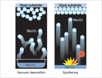
With vacuum deposition (left), thinfilm material is heated and evaporated to affix it to the substrate surface, so it is easy for foreign matter to enter, and for gaps to develop.
With sputtering (right), the thinfilm material is hit by ionized gas and bounced into position to form well-packed, smooth thinfilms free of foreign matter.
Nikon’s multi-layer thinfilm technology meets diverse industry needs.
Their exceptional durability makes them invaluable for use in space systems subjected to the rapidly changing temperatures and vacuums of outer space. Their low film stress means they can be grown on extremely thin glass substrates, even without substrates, such as in our substrate-less filters. Nikon will continue to develop and release new thinfilm products having new characteristics.
- *One billionth of a meter (10-9 meters).
Posted April 2003