Revolution will come to the world of lenses.
I am convinced that in the near future, a product will be introduced that changes the whole concept of lenses.
Your spectrum of project fields is very wide, from loupe to semiconductor manufacturing equipment. You are a manager of the optical design laboratory at the R&D headquarters of Nikon. What is your principal role?

In our laboratory, there are many specialists, who have already established careers as optical design engineers. You may be surprised to hear this, but professionals dedicated to optical design are not numerous. In this sense, our laboratory members are extremely important for the industry. Their subjects of study vary widely. For example, one may be dedicated to work directly connected to the present business of the company. Another will be concentrating on the future development of business in years to come.
What is the subject of your study?
Optical design is constantly advancing, as is any other technology. There are technologies that are not directly related to ours at all at this moment in time, but even among them, there are likely to be new technologies that may be important to our field of study in the future. I focus my efforts on a fundamental study of such new technologies.
Please tell us about such new technologies.
One of them concerns a light beam control via a structure artificially designed on the surface of or inside a material. Here is an example of a technology we employed for one of our products. It is the diffractive optical element (DOE)*1, the surface of which is designed with a sawtooth-shaped cross-section to create a diffraction*2 phenomenon. This innovation was employed in Nikon Media Port, UP.
You are not simply combining already existing materials to control beams, but creating new lenses, adding various new functions, isn’t this so?

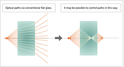
You are right. We can create tens-of-nanometers size patterns with our IC steppers and scanners. Each pattern is less than 1/10th the light wavelength in size. Traveling as electromagnetic waves, light behaves in certain ways. For example, a flat glass plate with a particular function incorporated can bend light like a lens. (See diagram)
So, how do you realize such possibilities?
As a matter of fact, in the long history of optics, various ideas have been proposed and theories established that support these ideas. Nevertheless, in many cases we could not say for sure whether they would be actually developed as products for the market. The technologies required were often not yet advanced enough to realize actual manufacturing. The recent evolution of microfabrication technology, however, helps some of these desk theories become hard reality.
It is my mission to take maximum advantage of current microfabrication technologies and materials, and explore new possibilities in micro-optics and nano-optics. If you ask when the results of my studies will be employed in actual practice, I’d have to say it still requires time because there are various issues and aspects we have to clarify, such as costs and production efficiency.
We experienced a big transition from film to digital in photography. Are you saying that a similar huge wave of a change is coming to the world of lenses?
Yes, I’m convinced that a new era is coming. Design methods will change. Until now, we have designed new lenses by changing materials or modifying shapes. But, in the not too distant future, we will employ new methods to design lens materials themselves. For example, we can create functions we desire in lenses by artificially forming structures of various patterns inside them.
Mr. Tanaka, you are dealing with the future of optical design.
Yes, but I do have a regret. Some 20 years ago, I created a progressive lens for eyeglasses. I developed the lens with a freeform surface*3. Prior to this development, I created the software necessary to design the lens itself. My regret is that I did not make further efforts to extend the use of this technology to other areas. Now, freeform surface design has spread everywhere. I wish I'd been able to utilize that software for a wider range of engineering applications two decades ago. Unfortunately, at that time, I had no latitude to think of adapting this software for use in other areas, because new tasks were always rushing in, one after another.
So as never to repeat this missed chance, I may need to make it my task to explore the new possibilities of existing technologies, while also attending to cutting-edge technologies.
- *1Diffractive optical element (DOE):
Generally, a lens changes light direction by refraction, while a DOE achieves this via diffraction. - *2Diffraction:
Waves of sound or light spreading around obstacles after passing small openings. - *3Freeform surface:
A freeform surface lens does not employ the axial symmetry design which is used for spherical and aspherical lenses.
