Conclusions can differ, depending on how you deliberate upon data.
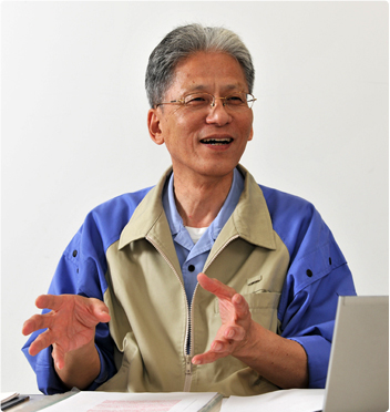
My turning point as a researcher.
When did you start research of thin films?
In May 1983, my ninth year at Nikon, I was dispatched to the Research Development Corporation of Japan, later renamed the Japan Science and Technology Agency, and stayed there for three and a half years. I was appointed as a researcher on glass and amorphous compounds. I engaged myself in the study of "the transparent magnetic thin film formed by the reactive ion cluster beam evaporation method." This project, directed by the Science and Technology Agency of the time, was my first step into thin film engineering technology. It was a very stimulating experience for me to work with many excellent researchers gathered there.
What did you gain from this experience as a researcher?
Experiments, examinations and hypothesis verification were repeated numerous times in this project. Through participating in the project, I developed an awareness of the importance of data far more than before, besides achieving a better understanding of the nature of materials. When you look at data, there's a great difference between the conclusion you come up with after 30 minutes of speculation and that which you arrive at after three hours' concentration. I eventually realized that it is also necessary to discard any data once you decide it is unnecessary, after you've closely examined it. My three and a half years at the institution taught me the importance of gaining a complete understanding of the data.
It was a project that had a huge impact on you, wasn't it?
The harvest I reaped here was that I discovered the direction I should take as a researcher. Meeting prominent researchers of certain fields helped me realize that those directions were not suitable for me. I discovered, instead, that I was cut out for solving problems and achieving a concrete goal through collaboration with other researchers. This was one of the most important turning points for me as a researcher.
The challenge of developing an optical thin film commenced.
When you returned to Nikon, you began to be involved with optical thin film development. How challenging was it?
I started development of an optical thin film in 1988. At that time, the light source of IC steppers and scanners was shifting from a mercury lamp with g line*1 to that with a shorter wavelength of i line*2.
The demand for a new optical thin film technology was increasing.
High-refractive-index materials with a larger absorption coefficient can't be used with shorter wavelength light sources. This leaves medium- and low-refractive index materials as the only options. We had to overcome this restriction and control the light, by elaborating the thin film designs and deposition technologies.
Did the scale of development grow as the wavelength of the light source became shorter?
We went on to develop optical thin films to be used with krypton fluoride (KrF*3) and argon fluoride (ArF*4) as those light sources with a shorter wavelength were employed. As development advanced, we became short staffed. We expanded our team by negotiating with other divisions that employed engineers with thin film knowledge and recruiting them. In the semiconductor industry, because technology is constantly advancing, severe competition takes place. Development must be undertaken systematically and at speed. Fostering engineers and organizing a skilled team is crucial.
- *1G line: Mercury light source with a wavelength of 436nm
- *2I line: Mercury light source with a wavelength of 365nm
- *3Krypton fluoride: Krypton fluoride excimer laser light source with a wavelength of 248nm
- *4Argon fluoride: Argon fluoride excimer laser light source with a wavelength of 193nm
Experience in the manufacturing division.
Please tell us about reforming the manufacturing division.
I was appointed in 2003 as the General Manager of the Lens Production Department, Production Technology Headquarters, Core Technology Center. This was my first appointment to the manufacturing division. There, I tried to create a lively workplace by adopting various projects including business and environment improvements. One of them was to encourage supervisors to initiate greeting their staff members, instead of waiting for staff members to greet them, which is the usual Japanese tradition. This verbal greeting, or aisatsu in Japanese, is derived from what is known as koekake, in which Zen Buddhist monks ask their apprentices how they are. Such greeting is essential for supervisors to check on their staff's condition. Other policies I adopted also overturned the status quo and accepted conventions. However, I gained the support of my staff by always being the first to follow such new policies.
How did you display your management skills in the Glass Division?
Following the Lens Production Department, I was transferred to the Glass Division. At that time, the size of LCD steppers and scanners was increasing as LCD TVs were becoming larger. The Glass Division was in charge of manufacturing large-scale LCD photomask substrates. There, I oversaw the entire business as the Division Manager, building on my experience in the Lens Production Department.
Did you encounter any problems?
I had a difficult time solving the issues of grinding, polishing and cleaning large-sized glass. The absolute requirement was to produce large-sized glass with no scratch larger than 2μm on the surface. It was a battle with the extensive surface and the weight. A series of unexpected accidents followed. Each time, we tackled the problem by considering the whole situation entailed in the mechanism of manufacturing, the stability of the equipment, the effect of gravity and the influence of the size, among other criteria. We identified point by point what was happening before our eyes, listed data, and solved these problems. When the first 10th-generation photomask substrates*, the largest at that time, were shipped to the client with the assurance of no scratches, we were extremely happy.
- *10th-generation photomask substrate: LCD photomask substrate of approx. 2m x 2m