

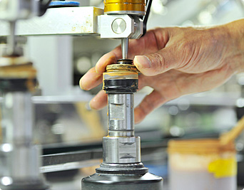
Tadashi Okawa
Lens Production Department, Production Technology Headquarters, Nikon Core Technology Center
Joined Nikon in 1975. He was assigned to work on polishing lenses for cameras and was subsequently responsible for lens-polishing for IC steppers and scanners. Appointed as a Nikon Master Craftsperson in 2007.
Mr. Okawa is currently engaged in polishing lenses used in the field image alignment (FIA) systems installed in IC steppers and scanners.
IC steppers and scanners expose the circuit patterns for ICs onto silicon wafers—the material for ICs. In order to produce a single IC, the reticle, which has a circuit pattern inscribed on it, is changed several dozen times and the circuit pattern is built up through repeated exposure. For this purpose, the silicon wafer and the reticule must be precisely aligned with one another and multiple sensors are used to gauge their respective positions. One of these sensors is the FIA system, which detects adjustment marks on the wafer by image recognition technology and corrects the position of the wafer or the reticle.
This positional alignment is carried out to a nanometer degree of precision (precision to one billionth of a meter). Obviously, the lenses in the FIA system must also be accurate down to the nanometer level. Mr. Okawa's technique is being put to good use in IC steppers and scanners, which are regarded as the most precise machines ever developed.
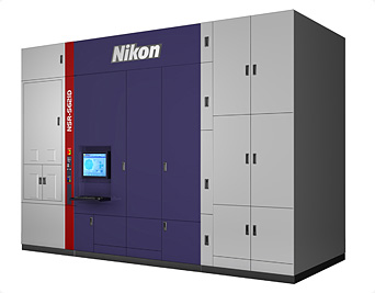
ArF Immersion Scanner NSR-S621D