4. Evolving into the next generation

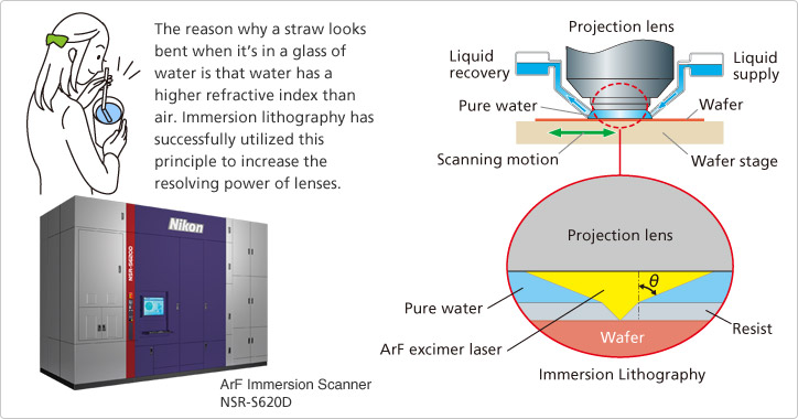
Since their advent, ICs have rapidly become smaller and an increasing number of functions can be achieved with them. As this evolution has progressed, Nikon has continued to develop lithography technologies with higher resolution capabilities to keep up with the ongoing miniaturization of ICs. With the progress of miniaturization, however, a theoretical barrier was reached that prevented existing lithography technology from handling the smaller sizes. The solution to this problem was Immersion Lithography Technology, which Nikon incorporated into its IC steppers/scanners.
Immersion lithography achieves a higher resolving power by filling the space between the projection lens and the wafer with purified water—the refractive index of purified water is higher at 1.44 than that of air (1.00). In immersion lithography, purified water itself is used like a lens. This technology makes it possible to overcome the aforementioned barrier and fabricate ICs that are smaller than 40 nanometers in size. This means that as many as 1,800 lines can be drawn within a space the width of a human hair.
ICs that have become highly integrated with immersion lithography technology are already being used in many electronic devices and electrical appliances, making our lives increasingly comfortable and convenient. High miniaturization of ICs also reduces power consumption, mitigating their burden on the global environment.
