3. Although small, ICs contain a host of Nikon technologies
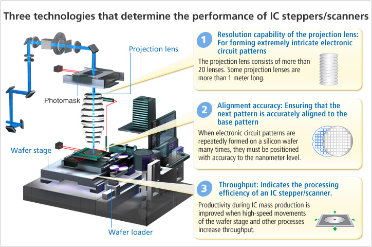
IC steppers/scanners require three key technologies and these determine their performance.
The first technology is "the resolution capability of the projection lens." The better the resolving power of the lens, the more intricate a circuit pattern can be when it is optically transferred. To improve lens performance, Nikon manages quality through an integrated system of production from the blending of raw materials for the lens to dissolving, grinding, coating, and assembly.
The second technology is "alignment accuracy." To produce a single IC, photomasks must be replaced tens of times and circuit patterns must be repeatedly etched in the exposure process. It is therefore of critical importance that the silicon wafer and photomask are perfectly aligned each time. Nikon uses multiple sensors to accurately position the photomask and silicon wafer.
The third vital component is "throughput." This technology is important when ICs are mass-produced. Throughput is an indication of productivity, which is expressed by the number of silicon wafers that can be exposed in an hour. To expose the maximum number of ICs on a single wafer and boost throughput, Nikon has developed the ability to move the stage that holds the wafer in position at extremely high speeds.
By combining these three technologies, Nikon has succeeded in making IC steppers/scanners that are described as "the most precise machines in history."