2. Fabricating high-precision, multifunctional ICs
-
1. Slicing a silicon wafer
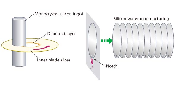
A cylindrical, high-purity silicon ingot is cut into discs to make silicon wafers with orientation notches.
-
2. Forming oxide film
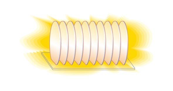
The silicon wafers are lined up and annealed in a furnace with the addition of oxygen and silicon gas to produce an oxide film on the surface.
-
3. Applying photoresist
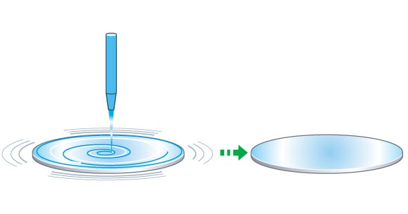
Next, a photosensitizing agent known as photoresist is applied to the surface. The silicon wafer is rotated at high speed during the coating process so that the photoresist is applied thinly and uniformly onto the wafer.
-
4. Varying photomasks
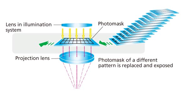
The various elements are formed on the silicon wafer by using different photomasks. Processes 3 to 8 are repeated several tens of times.
-
5. Exposing
An exposure unit called a stepper aligns the silicon wafer and the photomask, reduces the electronic circuit pattern on the photomask to a quarter or a fifth of the size through a lens, then projects light on the circuit pattern to pattern it on the silicon wafer. Exposure is done chip by chip, so this process is repeated hundreds of times over the entire wafer surface.
-
6. Developing
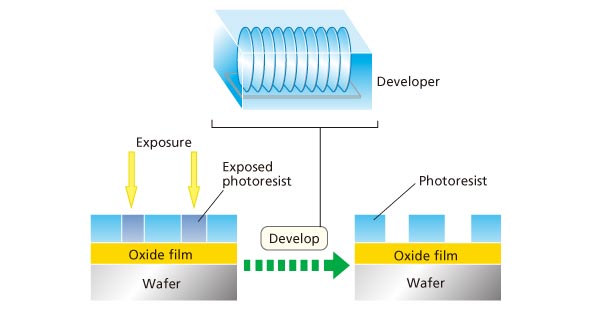
In the development process, the photoresist of the exposed areas is dissolved by immersing the wafer into a liquid solvent. The oxide film under the exposed areas is revealed.
-
7. Etching
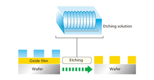
After the revealed oxide film has been removed, the remaining unwanted photoresist is removed to reveal the patterns.
-
8. Doping
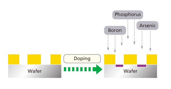
The transistors, diodes and other elements are formed on the silicon wafer by adding chemicals such as boron, phosphorus, and arsenic to the wafer in a furnace.
-
9. Wiring
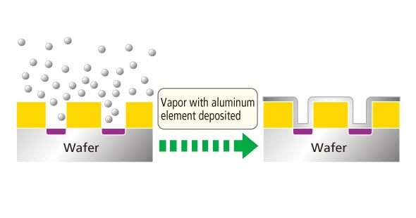
To connect the elements formed on a silicon wafer, aluminum is deposited onto the surface, and aluminum on unwanted areas is removed.
-
10. Dicing
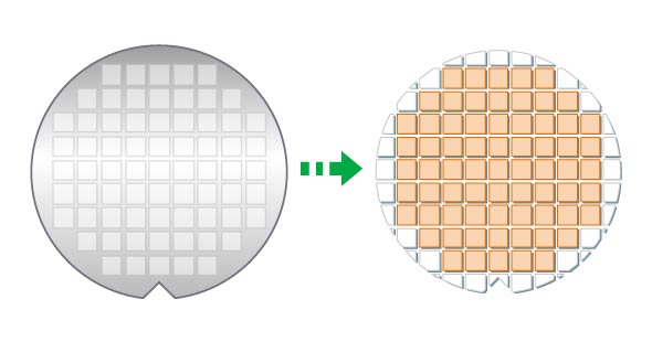
The chips on the silicon wafer are cut off one by one.
-
11. Bonding / Molding
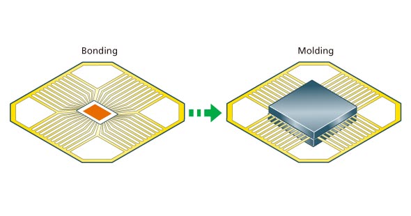
The chips and leadframes (the frame for connecting the chip to the terminals) are then connected via thin gold wires.
The chips are enclosed in synthetic resin or ceramic packages to protect them from shock and scratches. -
12. IC completion
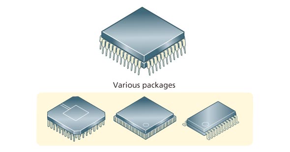
The frame section is removed and leads are shaped so that the IC can be mounted on a board.
ICs are made using IC steppers and scanners. An IC stepper/scanner is like a device that enlarges a photo. With photos, small images on film are enlarged and printed onto photographic paper, whereas in IC manufacturing, highly complex circuit patterns drawn on a photomask made of a large glass plate are reduced using ultra-high-performance lenses and etched onto a silicon disc known as a wafer.
If even a tiny bit of dust gets onto the lens or the wafer while an IC that requires extremely fine processing is being fabricated, it is not possible to etch the circuit accurately. It is therefore necessary to use a cleanroom where dust and dirt has been reduced to an absolute minimum. Workers in a cleanroom environment need to wear full-body garments to prevent dust or other foreign particles from getting onto the equipment.