The power of science advances the development of IC steppers and scanners.
Diverse technologies merge during the development of IC steppers and scanners.
So, it is Nikon’s continuous efforts that have been steadfastly improving the performance of its IC steppers and scanners.
It was in 1980 that Nikon first launched its IC steppers onto the market. After 30 years, the performances of the latest steppers and scanners are beyond comparison, and the microfabrication has dramatically advanced.
What’s the history of development of microfabrication in semiconductors?
Microfabrication in semiconductors basically involves how narrow (and close together) you can draw lines on ICs. The brightness of the projection lens and the wavelength of the laser source determine the quality of microfabrication. Let me outline a general path of progress in miniaturization. The first step is an improvement of the lens. You are asked to develop a brighter lens, which is merely a partial improvement. When you hit a limitation to lens development, you switch to shorter wavelength development. Employing a laser source with a shorter wavelength will improve the overall specifications, and help you go beyond the limit. In the past, the history of the wavelengths we used in microfabrication started with a 436-nm*1 g line, then a 365-nm i line, 248-nm KrF excimer laser*2. and 193-nm ArF excimer laser*3. We achieved this progression to shorter wavelengths at intervals of seven years or so.
Overcoming such limitations must have given you many obstacles to conquer.
A long list, indeed! (Laughs) Even though I can easily recognize what’s expected next by our industry, it’s quite another thing to tell whether or not I can actually realize it. When you start planning, many tasks emerge one after another. At the very start of a new project, we usually make a general assessment. When the success percentage is high, we invest tens of researchers and engineers on it, but if the percentage is low, we assign only a selected few. When you develop an IC scanner, you also need to develop related technologies side by side along the way. For example, if you employ a new wavelength laser source, you also need to find the lens material and photoresist that best match the wavelength. Accordingly, related peripherals must also be created. Many diverse technologies are required to innovate completely new IC steppers and scanners.
So for the successful development of IC steppers and scanners, you cannot just stay isolated in your particular research in the laboratory, can you?
Indeed. Professionals must gather together to successfully create IC steppers and scanners. Related departments work together to find the best solutions in close collaboration. Meetings to adjust differences are repeated until all the members come to an agreement. Specialists in various fields come together to contribute their latest knowledge and expertise. Through these combined efforts, the best machine of its generation can be realized.
Various types of expertise must cover a wide range of fields of science and technology.
During the development of IC steppers and scanners, almost all categories of science are involved: physics, precision machinery engineering, electronic engineering, information engineering and chemistry. A more detailed range of expertise includes: dynamics, electromagnetics, thermodynamics, continuum mechanics, machine design, electronics design, software design, geometric optics, wave optics, materials science, quantum mechanics, control theory, fluid dynamics and other various scientific fields of engineering and technology. As far as the immersion scanner is involved, certain knowledge of biotechnology is also required as the machine uses water. I wonder if there’s any other such product that requires this incredibly wide knowledge of science.
- *1nm: nanometer; 1/1,000,000,000 or 10-9 meter
- *2KrF excimer laser: Krypton fluoride excimer laser
- *3ArF excimer laser: Argon fluoride excimer laser
We knew the Nikon immersion scanner was a success even while it was still under development.
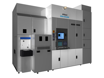
The NSR-S609B, Nikon’s first immersion scanner
Tell us about the immersion scanner. We understand that it employs an epoch-making method, in which exposure is conducted in completely purified water introduced between a projection lens and a wafer. When it was first launched onto the market, this machine surely made a strong impact on the industry. In particular, as a developer of the immersion scanner, you yourself must have experienced a great moment of realization.
The development of the immersion scanner was a great success and it guided us to even greater success in business. There is an untold story behind this achievement.
It sounds very intriguing. What was it?
As a matter of fact, preceding this immersion scanner, our team and myself had been strenuously developing another type of scanner. This ended, however, with the advent of the success of the immersion scanner. The other type of scanner we had been developing at that time employed an F2 laser with 157-nm wavelength as an optical source. The development of immersion lithography had started while we were still struggling with this F2 scanner. The technologies involved in the development of the F2 scanner had imposed upon us a high hurdle to conquer. Many difficult tasks to solve had also piled up. The one greatest problem to overcome had been the quality control of fluorite, which had hindered us from producing a projection lens that would satisfy our level of standards. While I was still struggling with the F2 scanner, I came across a technical paper on immersion lithography technology, written by a researcher at the Massachusetts Institute of Technology. It described the possibility of water-based immersion lithography with a 193-nm wavelength ArF excimer laser. It grabbed my attention in an instant. This was in the year 2002.
How did it influence you?
With the F2 scanner, we had to develop everything completely from scratch, lens materials, photoresists, and so on. On the other hand, almost every basic technical problem had already been solved with this ArF technology with 193-nm wavelength. It gave me an impression that all I had to do with this ArF scanner technology was simply add water to the original structure.
Even for us amateurs, it doesn’t seem very simple to add water to a precision machine.
The line width on circuits is inversely proportional to the brightness of a projection lens. When the NA or brightness of a lens is improved, the line width the lens creates gets narrower. In theory, the NA will never surpass the 1.0 barrier in the air. But when purified water is introduced in between a projection lens and a wafer, it does. This is the basic idea of immersion lithography technology. This theory had been acknowledged already for a long time, but there still remained the problem of how to handle the purified water. This was a barrier that was not easy to surpass. Nikon was already researching the possibility of using immersion lithography technology back in the 1990s, but this issue of how to actually deal with the purified water remained unsolved. The level of technology at the time could not readily give us a solution.
Then, it was the development of the local fill nozzle and tandem stage that solved the issue.
Yes, we combined the local fill nozzle with the tandem stage that was developed later. This helped maintain the productivity required for mass manufacturing, while controlling the purified water. In the design of the Nikon immersion scanner, purified water filling the space between a projection lens and a wafer must keep flowing without stopping. Even when a wafer is being replaced, the flow must never be interrupted. The continuous flow suppresses temperature rise, while removing impure substances generated during the exposures. We devised unique designs for the shapes of the local fill nozzle used at the openings that let the purified water in and out, and invented a new method to keep it flowing. Not a few hints were borrowed from the development work on the scanner with the F2 laser.

Would you tell us about that?
In the F2 scanner design, no air was allowed to enter the path the laser beam runs through. The air was completely purged, and nitrogen was introduced into the path of the laser beam. In the laboratory, the simulation studies with nitrogen were repeated many times to check fluidity. These simulation technologies introduced during the development of the F2 scanner by using nitrogen were optimally utilized in the development of our immersion scanner that uses purified water.
Did you have confidence that you would succeed even when you were still only halfway along the path to developing the immersion scanner?
I had a strong belief that this would be technology we could rely on. In the development of the F2 scanner, we encountered a new barrier at every turn of the path. On the other hand, with the immersion scanner, every obstacle was cleared at each stage, while the performance showed impressive progress as we moved forward. I was confident, I thought "This is it."