I ran through simulations mentally before development begins
The development of MTF test equipment: Making a huge impact in the photographic industry.
Tell me about this equipment — one of the most renowned products you designed. What is modulation transfer function (MTF) test equipment, designed to test a camera lens?
MTF is one of the methods used to evaluate camera lens performance. To explain MTF, one must understand how image qualities are generally judged. We need to consider what makes a good quality photo.
Well, I expect it might be the resolving power.
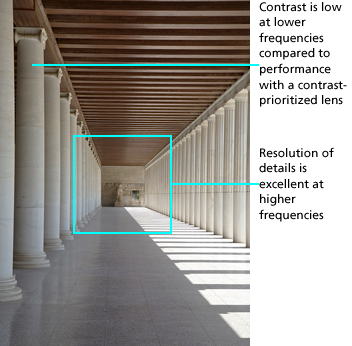
This matter is quite difficult to explain. Resolution is an index that describes how much small detail a lens can catch. Generally speaking, the smaller the details, the better the quality.
Showing finer details will not necessarily give the best quality of photo rendition?
Contrast also determines image quality. Even a low-resolution photo has a better image if it has improved contrast. MTF is one of the standards to evaluate how good a lens is considering the performance of contrast.
You were the first at Nikon to develop test equipment employing the MTF method.
The instrument that evaluates photo quality via MTF was already in existence at a laboratory. I decided to try and extend its use to a practical industrial level. This was around 1980.
It was just when the focus of camera lens design was shifting from resolution to descriptive powers. At Nikon, every lens inspection system line introduced this MTF equipment — in Japan, Thailand, and all Nikon's other mass production lines around the world.
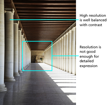
Contrast-prioritized lens
Resolution-prioritized lens
Nikon Fellow Nakamura's work helped improve the precision of IC steppers and scanners.

Did any other achievements impress you as much as the development of MTF test equipment?
The interferometer for measuring surface shape is the next most impressive, in my opinion. I developed it around 1983, and it was technology related to the measurement of spherical precision of a lens used in IC steppers and scanners.
It was also the first of this kind developed by Nikon.
The overall precision of lithography depends on the spherical precision of a lens at nano level. Measurement accuracy is crucial here. I regret to say, at that time Nikon had no inspection device of its own, and used an imported model. We were determined to develop our own.
How did you organize this project?
I took responsibility as project leader and developer of the mechanical design. I called for the best and brightest from every part of the company — electronics designers, optics experts, software developers, etc. — to form the ultimate project team at Nikon. I also asked for the participation of line engineers at factory sites. It took two years to complete the development of Nikon's own test equipment.
Were there differences of opinions? They were a collection of experts from many different fields of science.
The discussion was heated and excited, crossing lines of expertise with disputing opponents. Being experts, however, each considered opponents' arguments seriously, going back to the office with them to study. When they came back, it was with solutions. I found that what's important in this kind of project is to let each expert take responsibility of their own.
I expect there were many unforeseen problems.
The interferometer for length measurement was already there, but that for surface shape measurement was quite a new challenge. There were many problems to overcome. I remember that we continued our efforts on the last working day of the year, while other sections were holding a year-end party. Just then, we achieved the results we had long expected. We were overjoyed at the news. It is quite an unforgettable memory even today, after all those long years!
Was it very difficult when compared with other types of development projects?
Regarding levels of precision, those required for lithography are beyond comparison. However, the hurdles to be overcome in order to attain certain standards are always high at Nikon, with cameras or any other optical products. For example, with test devices for cameras, what is required is shorter test time, reliable performance, fewer malfunctions and easier maintenance. Development policy differs from one test product to another. Each test has its own unique issue to solve. This is at the same time exciting and a great challenge for a developer.
Have you ever felt that you'd hit a dead end?
Just for the record, let's say it never happened. (Laughter)
Of course, failures were countless.
How do you deal with that?
I have a set method in my way of planning. First, I schematize possible failures in my plan chart. I repeat simulation plans many times from beginning to end. I check possible failure points first. Then I prepare solution plans for all of them. I repeat a simulation method in my head until I am fully satisfied. As long as I know I have alternative plans beforehand, I am always confident that I can attain a goal.
You mean you include all the possible failures in your plan.
What's important is to never let failures remain as failures. I was pledged to obtain solutions no matter how long it took. I continued to search for answers until I found them. Nikon will not let you give up. It is vital to persevere until one discovers a way to attain the goal.