
The Ultra Micro-NIKKOR 105mm f/2.8, which was completed in 1962, was the first product for semiconductor manufacture that Nikon (then known as Nippon Kogaku K.K.) ever produced. This article describes the Ultra Micro-NIKKOR, which boasted the highest lens resolution in the world at the time.
A high-resolution lens first used for microfilm
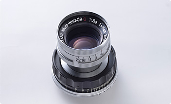
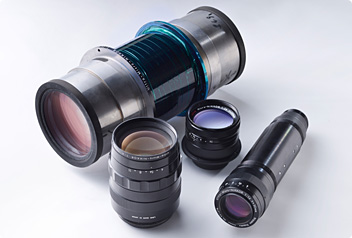
Micro-NIKKOR 5cm f/3.5 (the photo shows a Leica-mount lens)
Following World War II, microfilming systems (hereafter microfilm) were introduced to Japan from the United States. Microfilm involves the making of reduced-size copies (photographic reduction) of materials such as documents on 35mm format high-resolution film. This was to become popular at libraries and research institutions, as it enabled extremely compact storage of voluminous materials. However, as the photographic-reduction lenses that were imported were basically intended for the reduction of the Roman alphabet, they were incapable of taking clear photographs of typographically more complex kanji characters. This led to a demand for high-resolution lenses. In response to this, in 1956, Nikon added the Micro-NIKKOR 5cm f/3.5 to its series of S-mount interchangeable lenses.
A torrent of puzzling requests
In the very early 1960s, Nikon started receiving enquiries and requests from electrical and semiconductor manufacturers for high-resolution lenses for purposes other than use with microfilm. It subsequently became clear that these lenses were being used in the manufacture of photomasks. A photomask consists of a pattern describing the internal circuitry of a transistor. This pattern is transferred onto the transistor material to produce electronic circuits.
At that time, photomasks were produced as follows: a diagram of the electronic circuitry was photographically reduced to produce an intermediate negative, which was then in turn photographically reduced to produce the photomask. For this reason, there was a demand for high-resolution lenses that could photographically reduce detailed circuit diagrams accurately.
The development of special lenses for producing photomasks
As transistors gave way to integrated circuits (or ICs), the electronic circuitry of ICs was increasingly miniaturized, such that the resolution of off-the-shelf lenses was no longer sufficient. Accordingly, in March 1961, Nikon commenced development of a specialized ultrahigh-resolution lens for use in the production of photomasks—an effort led by the late Zenji Wakimoto *1 of the Optical Design Division.
- Lens resolution
The resolution of a lens is expressed in terms of the number of lines per millimeter that can be photographed using the lens (that is, the number of lines within a width of 1 mm). Assuming that there are no aberrations in the lens and that it can produce a perfect image, the upper limit for this parameter is obtained using the following formula:
Number of lines at maximum resolution = 1/1.22 λ F
λ is the wavelength of the light source (in millimeters) and F is the effective f-number. This formula shows that to achieve high resolution, a low f-number (high aperture ratio) and short light source wavelength are required.
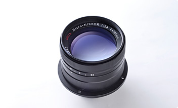
Ultra Micro-NIKKOR 105mm f/2.8
To obtain high resolution, a low f-number—that is, a high aperture ratio—is required. Using the technology of the day, it was difficult to correct aberrations in lenses with a high aperture ratio, and residual aberrations meant that doing so did not necessarily lead to better resolution. The fact that lenses for use in the production of photomasks also need to have a comparatively wide shooting range made aberration correction even more difficult, and some held the view that this was impossible to achieve.
However, this difficult problem was overcome through a combination of the design data that Nikon had amassed and the suggestion by the late Professor Jun Koana*2 of the Faculty of Science at the University of Tokyo, who proposed that it should be possible to correct various aberrations using monochromatic light (e-line with a wavelength of 546.1 nanometers). The lens that Nikon completed in August 1962 boasted a resolution of 400 lines per mm (an improvement over the 300 lines per mm that was regarded as the limit for photographic lenses) and a shooting range 24 mm in diameter. It was named the Ultra Micro-NIKKOR 105mm f/2.8.
- *1Zenji Wakimoto (1924-1996):
joined Nippon Kogaku K.K. in 1948, worked in the Optical Design Division and Camera Design Division, headed the Optical Division, and was appointed as a director of Nikon in 1977. In 1983, he received the Medal with Purple Ribbon for his development of ultrahigh-resolution lenses. - *2Jun Koana (1907-1985):
physicist renowned for his work in the fields of optical science and applied optical science. Supervised Mr. Wakimoto as a student. Served as professor at the University of Tokyo and at Sophia University.
Achieving a resolution of 1260 lines per mm—the highest in the world
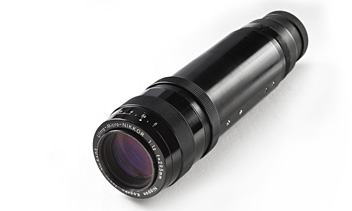
Ultra Micro-NIKKOR 29.5mm f/1.2
As the silicon wafers used in the production of ICs subsequently grew larger, photomasks also increased in size, and there was a need for lenses with a shooting range of 30-40 mm. As circuitry was also increasingly miniaturized, even higher resolution was required. Since there is a trade-off between high resolution and a wide shooting range, Nikon opted to aim for a restricted shooting range and high resolution.
Thus, a "sequential shooting" method was employed, whereby the pattern for the electronic circuitry was divided into narrow areas, which were photographed individually. Conversely, lining up a large number of electronic circuit patterns within a wide area and photographing them all in one go was known as a "simultaneous shooting" method.
In November 1964, Nikon completed the Ultra Micro-NIKKOR 29.5mm f/1.2, a sequential-shooting lens capable of resolving 1260 lines within a shooting range 2 millimeters in diameter. At the time, this represented the highest level of resolution for any lens in the world. Mr. Wakimoto also led the development of this lens, which employed a new optical design that included features such as a multilayer anti-reflective coating.
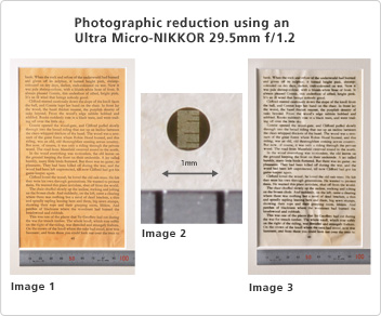
Using this lens, Professor Koana photographically reduced the 330-page text of the novel Lady Chatterley's Lover to the size of a 10-yen postage stamp of the day (approximately 12.5 mm square). He then further demonstrated that it was possible to enlarge this film back to the size of the original text and obtain the same resolution as that of the original. His results were presented at the Conference on Photographic and Spectroscopic Optics, which was held in September 1964 in Tokyo and Kyoto, where they received a tremendous response. The lens was selected by the Nikkan Kogyo Shimbun, Ltd., an industrial newspaper in Japan, as one of its Ten Best New Products of 1964, and in April 1965 Mr. Wakimoto and others involved in its development were awarded the Director-General's Prize by the then Science and Technology Agency of Japan.
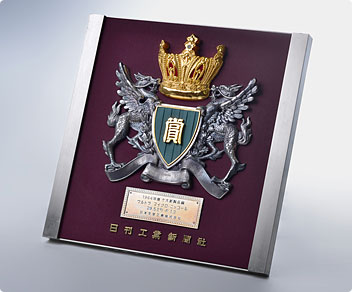
Prize shield awarded by the Nikkan Kogyo Shimbun, Ltd. to Nikon for the lens as one of the Ten Best New Products of 1964
The technology behind the manufacture of the world's highest-resolution ultrahigh-resolution lenses
Nikon expanded the Ultra Micro-NIKKOR Series, designing different lenses geared to specific properties such as wafer size, the required photographic magnification, and the photoresist.
The first step in the production of the Ultra Micro-NIKKOR lenses was the careful selection of the optical glass. Rigorous checks were performed for striae (deviations in the internal refractive index of the glass) and air bubbles, and annealing treatment was applied to properly limit internal distortions in the glass. The surface accuracy of the lens was then inspected to at least twice the degree of precision than that used for previous lenses.
In the assembly process, the engineers responsible for adjustment and inspection worked together, the resolution of the lens was verified by means of projection inspection, and further repeated adjustment was carried out based on the values produced by this inspection, so that the lens was then finished under ideal conditions. It was not possible to conduct this inspection properly while the factory was running, due to vibration, and stories are still told of how this work was carried out at lunchtime or during the night. Nikon marshaled all the manufacturing and inspection technology that it possessed to meet stringent standards of inspection.
From ultrahigh-resolution lenses to IC steppers and scanners
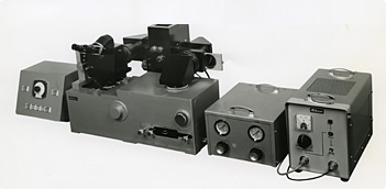
Projection Mask Printer equipped with an Ultra Micro-NIKKOR 225mm f/1.0
Projection area diameter: 50 mm
Resolution: 400 lines per mm
Projection magnification: 1:1
Light source: g-line (with a wavelength of 436 nanometers)
The lenses of the Ultra Micro-NIKKOR Series were highly acclaimed by the world's semiconductor and photomask manufacturers for their performance as specialized lenses for the manufacture of photomasks, and the series came to enjoy a monopoly in the global market.
Meanwhile, in 1967, Nikon's Camera Division and Machinery Division (as they were then called) began collaboration on the development of semiconductor manufacturing equipment that made use of the capabilities of these lenses. This was in response to suggestions from within Nikon that the company should develop such equipment. In 1969, Nikon completed its Projection Mask Printer, with the Ultra Micro-NIKKOR 225mm f/1.0 having been developed as the projection lens for this device. Nikon also invited electrical and semiconductor manufacturers to a product presentation at its Yokohama factory (now known as the Yokohama Plant).
This projection method was adopted on the present-day NSR Series of IC steppers and scanners. In other words, the Projection Mask Printer was the prototype for the NSR Series. Ultra Micro-NIKKOR lenses thus deserve to be remembered as the basis for the NSR Series of IC steppers and scanners (regarded as the most precise machines ever developed), which underpin semiconductor manufacturing both in Japan and throughout the world.