Lead-Free Electronics Technology
Sn-Pb eutectic solder, composed of tin (Sn) and lead (Pb) has been extensively used as a bonding material, for connecting wires in electronic equipment and mounting components on circuit boards, thanks to useful characteristics such as a low melting point, excellent wettability (how well it flows when liquid), and good bonding strength.
In recent years, however, the use of lead has been increasingly regulated around the world for environmental reasons.
The European Union, for example, was the first in the world to enact legal controls on the usage of hazardous substances, scheduled to be implemented on July 1, 2006.
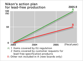
Nikon has established environmental preservation as a key corporate policy, and has been engaged in research and implementation to ensure that our products achieve the standards defined by this regulation as "lead-free circuit boards" by September 30, 2005.
The crucial points in "lead-free circuit boards" are the selection of lead-free bonding solder (cream solder for reflow, flow solder rods, and manual solder wire), and the bonding technology used.
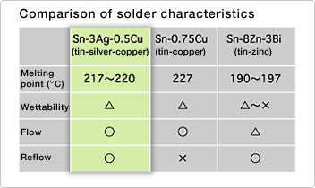
Most lead-free solder today falls into one of three types, all based on tin:
- Sn-Ag-Cu (tin-silver-copper) solder
- Sn-Cu (tin-copper) solder
- Sn-Zn (tin-zinc) solder
Most applications using lead-free solder actually use Sn-Ag-Cu, which is the most reliable of the three.
There are two major problems encountered when using Sn-Ag-Cu solder, however.
The first is that wettability, or how well the solder flows around components, is much worse then for conventional Sn-Pb eutectic solder.
This problem can be resolved to some extent through improvements in flux composition, and the use of a nitrogen atmosphere to minimize solder oxidation.
The second problem is that the melting point of Sn-Ag-Cu solder is about 220°C, much higher than the 183° melting point of conventional Sn-Pb eutectic solder.
In the mounting process the peak temperature is set above the actual melting point of the solder to provide a safety margin, and with Sn-Ag-Cu solder this peak temperature is so high that it poses a problem in terms of the heat resistance of the components themselves. Heat resistance varies according to the specific component involved, but most electronic components used today were designed for use with Sn-Pb eutectic solder, and so have a maximum heat resistance of about 240°C.
Achieving lead-free circuit boards will require lowering the peak temperature in the bonding process to a level matching the heat resistance of the electronic components, and minimizing the heating time.
Other problems are that the bond strength with Sn-Ag-Cu solder and reliability over time must be verified.
Let’s take a look at the actual bonding process.
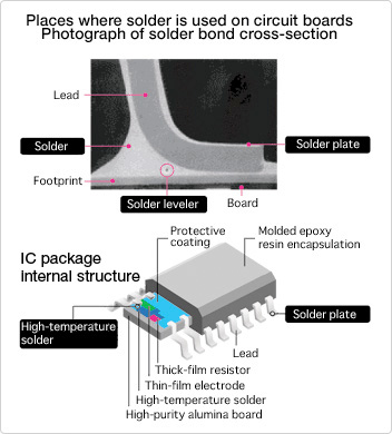
Components can be mounted onto circuit boards using manual soldering, with a soldering iron, or the flow soldering method where component leads are dipped into a bath of liquid solder. But for surface mounting in precision equipment, the most common method is reflow soldering.
In reflow soldering, cream solder is "printed" onto the electrodes located on the circuit board, the components set into place, and then the board passed through a reflow furnace (a type of electric furnace).
As the circuit board passes through the furnace, the cream solder is heated, melting to bond the component to the board.
The point here is that all leads on the board are heated uniformly. If temperatures are non-uniform, then when the temperature at one particular lead reaches the temperature needed to melt the solder, other places on the board may be at temperatures exceeding the heat resistance of the electronic components.
Optimal mounting conditions, ensuring temperature uniformity on the board and lowering of peak temperature, demand high reflow furnace performance and careful setting of the temperature profile, so that reflow furnaces normally have seven to nine heating/cooling zones. Board temperature uniformity cannot be assured by furnace performance alone, however.
Uniformity can be improved by careful control of the thermal capacity of the components, and by optimizing their layout on the circuit board. Nikon handles the complete process from design to mounting in-house, making it possible for mounting design engineers and production technology engineers to work together on researching board characteristics, component placement and other factors.
Nikon manufacturing covers a broad spectrum of production requirements from small-lot, multi-type production demanding high reliability to volume production, where quality control is crucial. Through our experience in manufacturing, we have mastered diverse mounting technologies, which we apply to our products.
The strength of Nikon expertise strongly advances the pursuit of lead-free, environmentally friendly mounting technology.
Posted July 2003