Carbon Nanotubes (CNTs)
Overview
Carbon nanotubes (CNTs) are the most remarkable new materials and are regarded as representatives for nanotechnology. CNTs are ones of carbon allotropes same as graphite (black lead), which is the material for pencil lead, fullerene and diamond but have characteristics in sequence of carbon atoms. CNTs did not capture the attention at all when they were discovered in 1970s, however CNTs started getting significant attention after their unique structures were identified in the early 1990s and their various properties related to the structures were revealed in the later 1990s. As the in characteristics, CNTs are strong yet have flexibility and are chemically stable. Also, the allowable current density is large and they are assumed to have the thermal conductivity equivalent to or more than diamond. Since CNTs significantly change their properties depending on their shapes, it is very important to selectively synthesize those that have the same properties, or to establish the technology which allows selection. The development race has been ongoing around the world.
Structure
Structures of CNTs are graphene sheets (carbon atoms are located at apexes of regular hexagons on two-dimensional surfaces) that are cylindrically curled. CNTs have high aspect ratios, namely the diameter is 0.4 nanometer*1 to several tens of nanometers and the length is 100 nanometers to several millimeters. CNTs are mainly divided into four types such as; (1) Single-walled carbon nanotubes (SWCNTs) which consist of one-layer graphene wall, (2) Double-walled carbon nanotubes (DWCNTs) which consist of two-layer graphene walls, (3) Triple-walled carbon nanotubes (3WCNTs) which consist of three-layer graphene walls and (4) Multi-walled carbon nanotubes (MWCNTs) which consist of more than three-layer graphene walls. The electronic properties significantly vary depending on the chirality (spiral) and the number of graphene walls. SWCNTs show both metallic and semiconducting properties depending on their chiralities.
One application of CNTs is the field emission display*2 which uses the property of electrons being emitted from CNTs only by applying low voltage in a vacuum. Also, CNTs are promising for supporting materials of catalysts in fuel cells, hydrogen storage, wiring of next-generation ICs, heat radiation, and electronic devices such as field effect transistors.
Selective synthesis of graphene walls
We have established the technology of selective synthesis for SWCNTs, DWCNTs, 3WCNTs and MWCNTs using an original Nikon method.
The transmission electron microscopy (TEM) is used for checking the number of graphene walls. Observation is conducted thorough every sample and the number of graphene walls of each CNT is checked from all the pictures taken.
Figs. 1 (a), (b) and (c) show the TEM images of "as-grown" SWCNTs, "as-grown" DWCNTs and "as-grown" 3WCNTs, respectively. Each image, when clicked, opens in a new window.
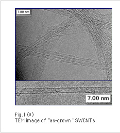
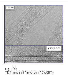
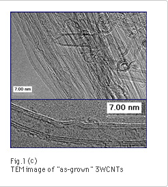
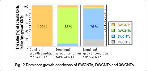
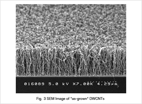
Fig. 2 shows the ratios of CNTs that consist of the specific number of graphene walls at deposition conditions of SWCNTs, DWCNTs and 3WCNTs. The ratio of selective synthesis of SWCNTs is 100%. The ratio of DWCNTs is 88% and the remaining 12% consists of the SWCNTs and 3WCNTs. The ratio of 3WCNTs is 76% and the remaining 24% mainly consists of DWCNTs and 4WCNTs.
Fig. 3 shows the SEM (Scanning Electron Microscopy) image of DWCNTs which grow vertically aligned on the quartz glass. Increasing deposition density of the active catalyst particles on the substrate allows the vertical aligned growth as shown.
Fluorination
Nikon is also involved in CNT fluorination research. In this research,
Fluorinated CNTs (F-CNTs) and amorphous*3 fluorinated CNTs (a-F-CNTs) have been synthesized and more variations of CNT properties have been created. For example, "a-F-CNT" is the world’s first CNT derivative.
Because fluorination changes dispersibility and the electrical property of CNTs, further applications are expected.
- *1One billionth of a meter (10-9 meters).
- *2Field emission display (FED) technology is similar in operation to CRTs in that a fluorescent screen is excited by a stream of electrons traveling through a vacuum. FED, however, is matrix-addressed, one entire row at a time with millions of electron-emitting cathodes. These emitters are a fraction of a millimeter (or up to 5mm in the case of high-voltage FEDs) away from the fluorescent screen, and they are produced by cold cathode emission.
- *3Solid materials crystallized with no specific atomic arrangement. This occurs when these layers are formed in a vacuum from vaporized materials as well as when materials are rapidly cooled down from a melting state.
Renewed April 2007