The outlook for the future: micro-machines and nano-processing
How could this technology be applied?
It could be used right away for measuring the shape of micro lenses. These are the minute lenses that are used in CD and DVD pickups. Another possibility is the measurement of micro-machine components. In addition, if a vibrating 8 µm probe were to have an even smaller 100 nm object adhere to it, the change in mass would cause the vibration frequency to change as well. Using this principle, it would probably also be possible to analyze ultra-microscopic substances in the air that cause environmental pollution. It can be assumed that if semiconductor lasers were arranged in an array, they were each used to trap a probe, and they were then operated simultaneously, it would be possible to investigate the concentration of a substance in the air in a short space of time. Since semiconductor lasers and the probes are built small, several hundred sensors could be mounted on a rectangular chip with sides of just a few millimeters. I wish someone would make one (laughs).
In addition, a variety of laser-trapping experiments are being conducted. For example, particles like sugar candy balls are also currently being manufactured using nano-technology. There are other experiments in which minute windmill-shaped thin-film diamond objects are being made and then rotated at high speed using optical radiation pressure. In the microscopic nano-level domain there is a whole world of physical phenomena in operation that are as yet not well understood. However, it is possible to make a hollow or dig a groove 8 nm deep in an object using microprobes and micro-tools.
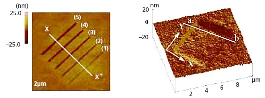
Examples of surface processing using laser trapping.
It is possible to form a gap or hollow several nanometers deep in the surface of an object.
Which is the most advanced country in terms of research in this field?
Image 4
Germany is the most advanced nation in nano-manufacturing and nano-measurement, probably followed by Japan and then the United States. However, there are various things involving laser trapping in air that only our laboratory is doing. We showed pictures of the probe introduced in this interview at a special laser trapping session held in the United States in August 2007, and these elicited an extremely strong reaction.
We are currently conducting experiments involving imparting rotational motion to a particle (or probe). Although it has proved extremely difficult to get a particle to move in an exact circle orbit, we are taking on the challenge in any case. For one thing, the position of a particle that has been trapped by imparting rotational motion to it is very stable. Even more interesting is the fact that when a probe that is moving in a circle orbit is brought close to the object to be measured, the circle orbit becomes an ellipse orbit due to the viscous resistance of the air, and the rotational axis aligns with the normal line from the surface of the object. As a result, both the coordinates and the normal direction can be ascertained simultaneously.
Ascertaining the normal line makes it easy to quickly move the probe so as to trace the object being measured. Since our laboratory building is located close to a civil-engineering laboratory, there are times when civil-engineering machinery is operating during the day, and even when we opt for the peace of the middle of the night, we cannot perform prolonged experiments, as vibration is a strict no-no when nano-precision measurement is being carried out. If we can improve the precision of our measurements, we would next like to reduce the time that it takes to perform measurements.
Thinking back, right from the start of this project we made unreasonable demands of Nikon (laughs). Initially we thought that they might turn us down. This was a device that no one had ever built before and keeping the design small in size must have been extremely hard. On top of that, Nikon seems to have put great effort into manufacturing all the components. Since Nikon was installing equipment devices that we had not used and whose features we did not properly understand, we had Nikon devise an adjustment mechanism that allows equipment to be swapped in and out. Incorporated into other equipment and measurement devices, the optical radiation pressure microprobe unit is likely to be in action soon.
Posted April 2008