X-ray irons out electronic flaws atProcess Sciences Inc.
Process Sciences Inc. (PSI) runs Nikon Metrology X-ray inspection to trace connectivity issues in electronic circuitry that otherwise remain hidden for the eye.
Using intuitive real-time X-ray imaging, PSI collaborates with OEMs and contract assemblers nationwide to reveal and resolve weak points in their PCB manufacturing processes.
XT V @ Process Sciences Inc. (USA)
By tracing connectivity issues in electronic circuitry, real-time X-ray allows PSI to assists customers in optimizing their electronics manufacturing processes.
- X-ray visualizes internal electronic flaws that otherwise remain hidden for the eye
- Intuitive real-time navigation through automatic position, angle and zoom adaptation
- Radiography insight drives efficient troubleshooting and cost-effective PCB repair
Literally looking into electronic boards and devices
Hidden electronic defects that remain undetected at first are often the topic of heated discussions between electronic designers and production engineers. As a consequence, additional prototype rounds are needed to sort out uncertainty about electronic system behavior and robustness. To avoid process delay and extra fabrication cost, electronics assembly suppliers and OEMs rely on PSI to verify their PCB prototype and production samples. PSI has the know-how to inspect, troubleshoot and repair PCBs at a cost that is only a small fraction of the fabrication investment for a new full-functional PCB prototype.
“Through electronics inspection at 3M, I learned about the extensive capabilities of Nikon Metrology XT V inspection systems,” says Stephen Schoppe, President of PSI in Leander, Texas. “For us, as an engineering and services company in the electronics industry, it is crucial to have the capability in-house to check PCB boards inside out. By visualizing connectivity failures in electronic devices and circuit boards, or between both, we are able to define the best way to readily provide a reliable fix. Insight into what really causes the problem is essential in optimizing customers’ electronics design and manufacturing practices.”
PSI’s 5,500 square foot engineering laboratory is equipped with electronics x-ray, rework equipment, microscopes, material validation systems, reballing stations, and other systems. Schoppe says that they organized x-ray inspection such that one system is dedicated to customers and the other to investigations performed by PSI. He marks that most customer projects are related to electronic connectivity issues including wire bonds, solder joints and through-layer vias.

On magnified x-ray images, voids and other defects in metallic surfaces immediately attract the attention

X-ray traces incomplete vias and helps create alternative routes for these open connections

Insight into electronic connectivity issues greatly reduces prototyping effort and manufacturing cost
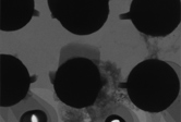
PSI engineers trace minuscule solder dendrites and voids scattered around the solder balls of BGA devices
Efficiently tracing and resolving connectivity issues
The XT V system enables us to literally look inside specimens, so that we can trace tricky defects that would otherwise remain buried under chip packages and PCB layers. Using angled imaging with high magnification, we reveal mysterious shorts in the form of minuscule solder dendrites and voids scattered around ball grid array (BGA) connections. In this case, we desolder, reball and reflow the device to reestablish correct and robust electronic connections.
Also incomplete vias are typically hard to trace without X-ray. “We use the system’s qualitative imaging and real-time X-ray capabilities to intuitively navigate through the layers of a PCB, by changing position, angle and zoom as desired. When detecting an open caused by an incomplete via, we investigate the surrounding internal structure to create an alternative route for the failing connection.”
Schoppe explains that image resolution up to 1 micron provides great insight into internal defects, such as inclusions found in solid metallic material. “In solid-state switches, for example, X-ray helped us identify irregularities inside the welded parts of the components. Similarly, we traced internal cracks in ceramic chip capacitors that were caused by electric stress.”
A growing quality threat in the worldwide electronics business are counterfeit chip dies produced cheaply in Far-East countries. PSI identifies an increasing number of counterfeit silicon that yields electronic performance risks. This is another reason why electronics OEMs have their boards verified by PSI before they pay their assembly suppliers.
Lower prototyping expenditure and manufacturing fail rate
Cisco, Flextronics, Schlumberger and St. Jude Medical are among nationwide customers that benefit from PSI’s X-ray related electronics services. Key in PSI’s services offering is supreme X-ray quality, which outperforms the imaging capability of previously installed systems on every single performance characteristic.
“The impact of top X-ray technology is huge,” Schoppe concludes. “Realtime displays showing angled views in highest resolution prove technical faults and support early defect discovery, reducing prototyping expenditure and manufacturing fail rate. Our technical expertise sharpened in advanced customer X-ray projects attracts new and repeat business for both services and consultancy.”
“Angled views in highest resolution prove technical faults and support early defect discovery, reducing prototyping expenditure and manufacturing fail rate.”
(Stephen Schoppe, President of Process Sciences Inc.)