For 80nm advanced devices incorporating the world's highest N.A. lens Announcing sale of Nikon's Step-and-Repeat Scanning System NSR-S307E
July 8, 2003
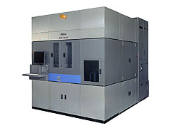
Nikon Corporation (President: SHIMAMURA, Teruo) has developed the Step-and-Repeat Scanning System NSR-S307E, a lens-scanning ArF excimer stepper for mass production of 80nm advanced devices incorporating the world's highest N.A. lens, and will commence sales in October 2003.
The NSR-S307E incorporates the world's highest N.A. (N.A.O.85) projection lens, for the ArF excimer laser (193nm wavelength), and uses a newly developed body to significantly improve throughput performance and alignment accuracy.
Sales Summary
| Product name | Nikon Step-and-Repeat Scanning System NSR-S307E |
|---|---|
| Price (excluding tax) | About 2.3 ~ 2.5 billion yen (varies by spec or configuration) |
| Sales launch date | October 2003 |
Development Background
Progress continues on increasing the density of VLSI chips, the foundation of the IT revolution, and today we are moving to the production of 90 nm rule devices. Nikon released the world's first lens-based scanning system, the NSR-S201A, in April 1995.
Since that time, the Nikon lens-scanning stepper has won consistent praise from semiconductor manufacturers around the world for its performance and reliability, and more than 600 i-line, KrF excimer laser, and ArF excimer laser models have been shipped.
This latest market entry, the NSR-S307E, incorporates a low-aberration projection lens with the world's highest N.A. (N.A. 0.85), in combination with the ArF excimer laser, to mark a further advance on the NSR-S306D projection lens shipped for the first time in March, for mass production of 80nm devices. Furthermore, the newly developed body has dramatically improved overlay accuracy and throughput performance. Throughput is now 112 or more 300mm wafers per hour, and 160 or more 200mm wafers per hour.
Major Performances
| Resolution | 80nm or better |
|---|---|
| N.A. (Numerical Aperture) | 0.85 |
| Light source | ArF excimer laser (193nm wavelength) |
| Reduction ratio | 1:4 |
| Exposure field | 26 X33mm |
| Alignment accuracy | 16nm or better (M+3σ) |
| Throughput (per hour) | 300mm wafers : 112 or more wafers 200mm wafers : 160 or more wafers |
Major Characteristics
- World's highest N.A. (N.A. 0.85) projection lens
Incorporates an advanced-performance N.A. 0.85 reduction projection lens, the world's highest, in combination with an ArF excimer laser, to achieve mass production of next-generation 80nm devices. Suitable for mass production of increasingly microscopic next-generation DRAMs and MPUs, etc.
- Higher throughput (processing performance) and improved alignment accuracy
A newly developed body achieves further improvements in throughput. Throughput is now 160 or more 200mm wafers per hour (an improvement of about 19% over the previous model), and 112 or more 300mm wafers per hour(an improvement of about 32% over the previous model). Alignment accuracy is also up by about 20% over the previous model, achieving a maximum accuracy of 16nm.
- The information is current as of the date of publication. It is subject to change without notice.