Bringing the Power of DUV Scanners to Mix-and-Match Start of Sales for Nikon Step-and-Repeat Exposure System NSR-SF120
July 11, 2002
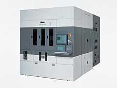
To create the most effective system for non-critical layers of next-generation DRAMs and MPUs, Nikon Corporation (SHIMAMURA, Teruo, President) has developed and will begin selling a new i-line scan field stepper, the NSR-SF120.
The NSR-SF120 is designed to realize superior cost performance in a mix and match strategy with Nikon KrF excimer laser scanners, which are now the main systems in state-of-the-art semiconductor fab lines.
The NSR-SF120 achieves a high resolution of 280 nm or better on a large exposure field of 25 x 33 mm.
The system boasts a high throughput of 100 wafers/hour or more for 300 mm wafers, and 120 wafers/hour for 200 mm wafers.
Sales Overview
| Product Name | Nikon Step-and-Repeat Exposure System NSR-SF120 |
|---|---|
| Price | Approx. 560 million Japanese Yen (Price depends on specifications) |
| Sales Inception | July 2002 |
| Expected Unit Sales | Approx. 50 units in first year |
Development Background
Nikon now sells the NSR-S204B and NSR-S205C systems used in the state-of-the-art semiconductor fab lines. These systems support the increasingly tight design rules as the industry accelerates from 150 nm to 130 nm applications. Starting this spring, Nikon began taking orders for the NSR-S306C, which enables 100 nm or better resolution with the world's first ultra-high N.A. (0.78) reduction projection lens and an ArF excimer laser.
Nikon was the first in the industry to develop a new-concept i-line stepper that focused on mix-and-match with lens-scanning type KrF excimer steppers in state-of-the-art semiconductor production lines. Nikon began accepting orders for this stepper, the NSR-SF100, in January 2000. This system is optimal for exposing the non-critical layers, which comprise roughly half of the approximately 20 layers of a device. With the same reduction ratio as the scanner, adequate resolution and high throughput, this exposure system is highly valued for its superior total balance and cost performance, which improve productivity and contribute to reducing total capital costs.
The NSR-SF120 being announced now enables a leap in resolution to 280 nm or better, by means of a newly developed high-N.A. reduction projection lens. The system can effectively expose non-critical layers in the 130-100 nm generation, and offer high throughput for the 300 mm age.
Main Features
- Large Exposure Field, High Resolution, High Throughput
The stepper provides the same large 25 x 33 mm exposure field as a scanning type system, and achieves high resolution of 280 nm or better by means of the newly-developed high-N.A. (0.62) reduction projection lens (compared to previous Nikon systems with N.A. of 0.52, and resolution of 400 nm). Furthermore, for 300 mm wafers, which are central to production line environments, industry-leading throughput of 100 wafers per hour or more has been achieved (a 25% over previous Nikon systems.)
- Optimal for Mix-and-Match
The NSR-SF120 is designed to operate in a similar manner as the scanning-type KrF steppers NSR-S204B, NSR-S205C, and NSR-S206D, as well as with the ArF steppers NSR-S305B and NSR-S306C. Not only does it support design rules of 130 nm, but will also support future 120 nm semiconductor mass production lines, and furthermore, as a mix-and-match exposure system supporting 100 nm lines, it will contribute greatly to mass production that will probably start by using scanning-type ArF excimer steppers.
Main Specifications
| Resolution | 280 nm or better |
|---|---|
| N.A. (Numerical Aperture) | 0.62 |
| Light Source | i-line (Wavelength 365 nm) |
| Projection Magnification | 1:4 |
| Exposure Field | 25 x 33 mm |
| Alignment Accuracy | 35 nm or less (M+ 3 s) |
| Throughput | For 300 mm wafers, 100 wafers/hr. or more For 200 mm wafers, 120 wafers/hr. or more |
- The information is current as of the date of publication. It is subject to change without notice.