High-throughput KrF scanner featuring an ultra-high N.A. lens Start of Sales for Nikon Step-and-Repeat Exposure System NSR-S206D
July 11, 2002
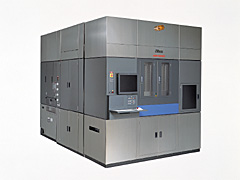
To support mass production of cutting-edge devices with 110-nm or better design rules using a KrF excimer laser, Nikon Corporation (SHIMAMURA, Teruo, President) has developed the NSR-S206D.
This new stepper incorporates a lens-based scanning system, an ultra-high N.A. lens, and a KrF excimer laser.
The NSR-S206D is the first system in the world to be equipped with an ultra-high N.A. lens (N.A. 0.82) that supports KrF excimer lasers (248-nm wavelength).
It provides high throughput of 88 wafers per hour or better for 300-mm wafers, and 147 wafers per hour or better for 200-mm wafers.
Sales Overview
| Product Name | Nikon Step-and-Repeat Exposure System NSR-S206D |
|---|---|
| Price | Approx. 1,200 million Japanese Yen (Price depends on specifications) |
| Sales Inception | July 2002 |
| Expected Unit Sales | Approx. 80 units in first year |
Development Background
VLSI silicon chips, which are the basis of the IT revolution, know no bounds when it comes to increasing integration. Today, mass production of these devices is shifting from 150 nanometer to 130 nanometer design rules. In step with this trend, Nikon unveiled the first lens scanning type system in the world, the NSR-S201A, in April 1995. Since then, Nikon's lens scanning type systems have received high marks for performance and reliability from semiconductor manufacturers throughout the world, resulting in shipments of over 500 units to date, including i-line, KrF excimer laser, and ArF excimer laser models.
The NSR-S206D being introduced now features the world's first ultra-high N.A. (N.A. 0.82), low aberration projection lens which can realize mass production of devices with design rules of 110 nm or better, using a KrF excimer laser. For device manufacturers who are actively working to reduce costs, this fulfills their need for "increased miniaturization with KrF."
Main Features
- Ultra-High N.A. Projection Lens (N.A. 0.82)
The world's first system to be equipped with an ultra-high N.A. (0.82) reduction projection lens that achieves a resolution of 110 nm or better. This enables mass production of next-generation devices below 110 nm with a KrF excimer laser.
- Improved Throughput (Process Capability)
Using a 4 KHz-30W laser, throughput has been further improved: at least 147 wafers/hr. for 200-mm wafers, now the dominant standard, and 88 wafers/hr for 300-mm wafers, which are used in production line environments. This represents an approximately 5% improvement over previous Nikon systems.
- Further Improvement of Alignment Accuracy
To support the ever-higher resolution, alignment accuracy has leaped from 30 to 20 nanometers.
Main Specifications
| Resolution | 110 nm or better |
|---|---|
| N.A. (Numerical Aperture) | 0.82 |
| Light Source | KrF Excimer Laser (Wavelength 248 nm) |
| Projection Magnification | 1:4 |
| Exposure Field | 25 x 33 mm |
| Alignment Accuracy | 20 nm or less (M+ 3 s) |
| Throughput | For 300 mm wafers, 88 wafers / hr. or more For 200 mm wafers, 147 wafers / hr. or more |
- The information is current as of the date of publication. It is subject to change without notice.