The Optimal Stepper Solution for Mass Production of High Definition Displays Start of Sales for Nikon Flat Panel Display Exposure System FX-801M
October 28, 2002
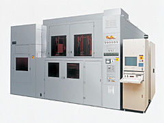
Nikon Corporation (SHIMAMURA, Teruo, President) has developed the Flat Panel Display Exposure System FX-801M. Sales of the system are planned to start in December 2002.
Using low-cost 6-inch reticles with decreased fabrication errors compared to large masks, the FX-801M transfers the reticle pattern to the entire glass plate with a step-and-repeat system. This flat panel display exposure system excels at providing superior cost performance in the mass-production of multiple product lines and the fabrication of higher definition liquid crystal displays (LCD) using low-temperature polysilicon and other technologies. While maintaining the resolution of earlier models, the FX-801M is also able to support increased plate sizes.
The new system can therefore achieve even more efficient mass production and so contribute to improving productivity.
Sales Overview
| Product Name | Nikon Flat Panel Display Exposure System FX-801M |
|---|---|
| Price | 575 million Japanese Yen (Differs depending on specifications) |
| Sales Inception | December 2002 |
| Expected Sales Volume | 10 units in first year |
Development Background
Thin film transistor (TFT) active matrix LCDs created a market for notebook computer displays, and their adoption for desktop and TV monitors has rapidly expanded that market.
Global LCD sales in 2001 exceeded 2 trillion Japanese Yen, and TFT systems accounted for more than 70% of those sales. There are increasing demands for brighter images and more natural video pictures, and advancements have been made so that video functions are common on cell phones and car navigation screens. Devices used in highly functional TFT LCDs are moving to the use of low temperature polysilicon (poly-crystalline), which has a charge-carrier mobility about 100 times that of amorphous silicon (non-crystalline).
While expanding its applications to support 730 mm x 920 mm plate sizes, the FX-801M also achieves superior resolution and overlay accuracy by adopting the stepper method and 6-inch reticles used to manufacture semiconductors. On small and medium-size panel production lines, the new system is capable of flexible production with high precision and superior cost performance.
In addition, a successor to the FX-702J (resolution: 1.5 um) is under development that will share plate size support for the mix & match environment in the low-temperature polysilicon TFT fabrication process and also be capable of simultaneously transferring patterns for even more highly functional driver ICs.
Main Features
- Large Plate Applications Using Stepper Method
The new model supports large 730 mm x 920 mm plate sizes (earlier models: 600 mm x 720 mm).
This capability means the FX-801M can fabricate 294 panels (2-in. panels) or 84 panels (4-in. panels) from one plate. - Fabrication of High Accuracy LCDs Achieved
6-inch reticles, which are indispensable in fabricating high accuracy LCDs, were adopted.
By adopting reticles used to manufacture semiconductors, not only were patterning errors during reticle fabrication reduced, but also alignment accuracy was improved to 0.4 µm or lower. - Superior Cost Performance
The reticles adopted not only provide high accuracy exposure, they are also optimized for multi-model production to reduce costs.
These advantages bring about superior cost performance capabilities. In addition, options enable the reticle library to handle up to 44 reticles.
Main Specifications
| Resolution (L/S) | 3µm |
|---|---|
| Exposure field | 132mm x 132mm |
| Exposure wavelength | g-line (436nm) and h-line (405nm) |
| Projection Magnification | 1.25 x |
| Alignment Accuracy | 0.40 µm (3s) or less |
| Maximµm plate size | 730mm x 920mm |
| Reticle Size | 6-inch |
| Tact time (30 mJ/cm2) | 89 sec. (42 shots) |
- The information is current as of the date of publication. It is subject to change without notice.