Achieving sub-0.1µm high resolution with high productivity Development of Electron Optical System for EB steppers
January 1999
Nikon Corporation, in collaboration with IBM Corporation, has successfully demonstrated feasibility of an electron optical system for EB steppers, which allows for extremely high productivity IC manufacture of sub-0.1 µm (= 100 nm) minimum pattern linewidth.
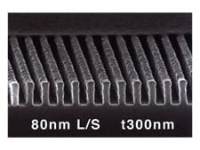
(Photo : SEM photo of 80 nm Line and Space test pattern printed with the electron optical system)
Consistent with a sub-100 nm design rule, predicted to be in production on a full scale in 2006 A.D., the proposed system will be capable of printing high performance MPUs and 16G DRAMs, which have approximately 250 times more memory capacity than currently with the mainstream 64M DRAMs, with throughput of forty or more 200 mm wafers per hour (about twenty 300 mm wafers).
What differentiates this system from "direct-write method" electron-beam exposure systems is that circuit patterns are demagnified and projected onto a wafer while being scanned in the same fashion as optical scanning steppers, which are currently in use for IC manufacturing process.
Background of the Development
ULSI has been steadily progressing towards higher density : mass production of 256M DRAMs has already started, and research and development of 1G DRAMs for future mass production is being actively conducted.
The trend for smaller feature sizes will continue, and by the year 2006 a sub-100 nm design rule could be employed, and a prototype for 16G DRAMs, which have approximately 250 times more memory capacity than currently with the mainstream 64M DRAMs is predicted to appear. (16G DRAMs will hold the equivalent of the amount of information that will appear in every edition of a japanese daily newspaper for the next 4 years.)
Responding to the demand for higher density by shortening the wavelength, steppers (reduction-projection exposure systems), which hold the key to higher density ULSI, went through the era of the g-line (wavelength = 436 nm) and the i-line (wavelength = 365 nm) light source.
These use high-pressure mercury(Hg) lamps as the light sources.
Now, the KrF excimer laser (wavelength = 248 nm) is about to become the main source for mass production.
For research and development of the next generation manufacturing process, steppers employing the ArF excimer laser (wavelength = 193 nm) are about to be in use and are expected to achieve resolution down to approximately 100 nm through future improvements in lenses and photoresist.
Nikon is involved in the following technologies that are expected to realize resolution of sub-100 nm :
- Reduction-Projection Exposure That Uses a Shorter Wavelength Laser such as the F2 Excimer Laser (Wavelength = 157 nm) as its Light Source
Since this technology is on the lines of the extension of current exposure technology in terms both of the exposure system's structure and the IC manufacturer's fabrication process, previously acquired expertise can be applied to it.
It is expected to have the high throughput that comes from optical exposure.
While there are still technical problems with lens materials and coatings, Nikon has been proceeding with studies of reduction optical systems that combine lenses and mirrors. - EUV Exposure
EUV exposure is also known as EUVL ( ExtremeUltra Violet Lithography) since it is a reduction -projection exposure technique using a wavelength in the extreme ultraviolet range (wavelength = 13 nm).
Development of technologies such as a reflective optical system that uses layered atomic level films and a light source that uses extreme ultraviolet generated from plasma created with laser light energy is underway.
Nikon joined the japanese "Association of Super-Advanced Electronics Technologies (ASET)", a research organization for the next generation electronics technology, in September 1998 to advance research and development in this area. - Exposure Using Electron Beam
In this system, circuit patterns are exposed on a wafer using an electron beam.
Electron-beam exposure systems have long been known for the ease with which high resolution can be obtained.
They are already in use in fabrication of advanced ICs in small lot sizes (such as ASICs) and in the research and development of the next generation of DRAMs and MPUs.
Development that focuses on increasing the throughput of future lithography technology is also underway.- 3.1. Electron Beam Direct-Write Method (Current Commercial Systems)
An electron beam generated by an electron gun illuminates a reticle having 20 to 100 types of patterns representing repetitive parts of the circuit patterns, and an electron lens using magnetic fields produces an image demagnified by a factor of 10:1 to several times that value.
A single shot exposes a single pattern within a rectangular area up to several µm square on a wafer.
The entire plane of the wafer can be written by stitching the circuit patterns sequentially with electron beam deflections of several millimeters and movement of the wafer stage according to the design data.
In the latest systems, a throughput of three to ten 200 mm wafers per hour. has been achieved with resolution of 150 nm. - 3.2. Electron Beam Reticle Projection Method (Under Development)
This method is being developed with a view to dramatically increase throughput.
As in the optical-system scanning steppers used in current semiconductor fabrication processes, circuit patterns on a reticle are printed onto a wafer through reduction projection while scanning with an electron beam.
- 3.1. Electron Beam Direct-Write Method (Current Commercial Systems)
The EB design whose concept was successfully tested through joint development with IBM Corporation, is based on the basic principle of image formation by this reticle projection technique.
IBM's electron beam technology enables a high current and a large deflection electron lens, thereby realizing this history-making EB stepper with dramatically improved throughput.
It is targeted to expose over forty 200 mm wafers per hour (or about twenty 300 mm wafers) at high resolution below 100 nm.
Nikon aims to commercialize the system as one of successors to the ArF exposure systems.
Overview of Nikon EB Stepper
A 1 mm square electron beam generated by an electron gun illuminates on a reticle (original circuit pattern), and an electron lens produces a 4 : 1 demagnified image.
One shot exposes a single pattern within an area of 250 µm square on a wafer.
The complete circuit pattern is exposed and stitched by scanning the reticle and wafer synchronously through the illumination with velocities of the reticle stage and the wafer stage in the ratio of 4 : 1 and by electromagnetically deflecting the beam by 20 mm on the reticle (5 mm on the wafer).
Principal Features
- Dramatic Increase in Throughput while Maintaining High Resolution
Novel designs and manufacturing technologies have been used to develop a new electron gun and electron lens system.
The extremely low aberration and low distortion electron lens enables exposure to be done with very large electron beam compared to conventional electron-beam exposure systems.
These larger electron beam greatly reduce the Coulomb effect*, allowing batch exposure of large areas at high current while maintaining high resolution.
As in current scanning steppers, a circuit pattern on a reticle (original circuit pattern) is demagnified by 4 : 1 and projected onto a wafer in this system.
The system is capable of exposing a 250 µm square area per shot, which represents 2,500 times larger exposure area than the conventional methods (See. 3.1.).
With the large deflection range, the exposure time is greatly reduced, thereby dramatically increasing throughput.
- *"Coulomb effect" :
A phenomenon where the electrons in the beam repel one another, leading to blurring of the beam.
Since the Coulomb force is inversely proportional to the square of the distance between electrons, the more concentrated they are, the greater the effect is.
Repulsion of electrons results in "beam blur" which adversely affects resolution.
Naturally, an electron beam with less size limits the amount of current to be given, thereby lowering throughput.
- The information is current as of the date of publication. It is subject to change without notice.