

An electronic microscope view of influenza viruses (brown) budding from host cells (green). XFEL enables observation of the precise molecular structure of a virus protein. In addition, it lets you observe which part of a protein is in action and how it works.
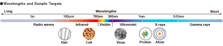
Just as X-rays can be used to observe massive objects that are light years away from the Earth, they can also reveal incredibly small objects that surround us. However, we cannot resolve objects that are smaller than the wavelength of the light illuminating them. Using groundbreaking X-ray technology, Japanese scientists are shining light on the mystifyingly small world of molecules and atoms — and making discoveries as dramatic as anything found in outer space.
Shining New Light on the Atomic Level
Most scientific achievement is built upon previous successes, prompting Sir Isaac Newton to remark, famously, “If I have seen further, it is by standing on the shoulders of giants.” Today, Japanese researchers are indeed seeing further, thanks in part to the successes of the Super Photon ring-8 GeV, or SPring-8, at Harima Science Garden City in Hyogo Prefecture.
The SPring-8 facility, in operation since 1997, delivers the world’s most powerful synchrotron X-ray radiation — radiation produced when electron beams, accelerated to nearly the speed of light, are forced to travel in a curved path by a magnetic field. In other words, SPring-8 produces brilliant light that researchers can use to study very small objects, such as structures within cells.
As powerful as SPring-8 is, its X-rays cannot take scientists into the tiniest realm of life, the world of atoms. The X-ray Free Electron Laser (XFEL), also at Harima, however, can. Because XFEL’s light is so intense, like none ever produced before, researchers can employ it to observe individual atoms and molecules.
“The radiation of SPring-8 was a lamplight compared with XFEL,” says Dr. Tetsuya Ishikawa, director of the RIKEN Harima Institute and the SPring-8 Center. “XFEL takes research to a whole new level. It is far brighter than SPring-8 — about a billion times brighter — enabling observation of chemical transformations at the atomic or molecular levels. We can observe natural phenomena and life activities as they happen.” Perhaps this is why XFEL has been called the “dream beam.”
Taking XFEL One Step Further
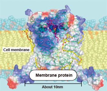
More than half of all drugs used today are designed to work with membrane proteins.
(Illustration: Courtesy of RIKEN)

The SACLA (oblong) and SPring-8 (round) facilities.
(Photo: Courtesy of RIKEN)
In 2006, after five years of research and development, the SPring-8 Angstrom Compact Free Electron Laser (SACLA) at Harima was selected as one of the National Critical Technologies to be included in Japan’s third Basic Program for Science and Technology. “SACLA is a compact, stable and highly reliable X-ray laser light source,” Dr. Ishikawa explains. “It includes some unique ideas that were born as a result of the SPring-8 accelerator.”
At SACLA (pronounced “sakura,” which means “cherry blossom” in Japanese), free electron beams are generated by electronic guns, and then accelerated to almost the speed of light. The beams pass through arrays of magnets — 5,000 of them — and emit X-rays with synchronized wave phases. During trial operations, a test at SACLA generated a laser with the world’s shortest wavelength of 0.063nm. This paved the way for full operational status in March 2012.
Dr. Ishikawa says that more than 500 leading Japanese manufacturers participated in the project. “The equipment is extremely sensitive; the beams must run within an error limit of microns. Very strict standards are required at the facility.” SACLA can be used in tandem with SPring-8 and linked to the K computer*, a supercomputer in Kobe, enabling even more research, data collection and analysis.
But what are the practical research applications of SACLA? Dr. Ishikawa says, “Any technology that enables us to see or analyze the nano world will become important in wider fields of industry.” This includes analyzing protein structure, particularly membrane proteins, which regulate the passage of substances in and out of cells. Most drugs today function by acting upon membrane proteins. “We expect to discover the mechanism for this,” Dr. Ishikawa says, “so we can understand the phenomena of life and create more effective pharmaceutical products.” SACLA might also be applied to study chemical reactions that could lead to the development of materials that support a low-carbon society, or employed to focus on finding a photosynthesis mechanism that could combat global warming or enhance agricultural techniques.
- *The K supercomputer was developed by RIKEN and collaborators. In 2011, it ranked twice in the TOP500 List of the world’s most powerful supercomputers. The K is also one of Japan’s National Critical Technologies.
(Information/material: Courtesy of RIKEN)
Invisible Rays Lead to Visible Improvements on Earth
There is a certain irony about X-rays: We cannot see them, but they have allowed us to see incredible things. From the far reaches of space, where hot, turbulent regions abound with gases and dark matter, to the “secrets” of paintings and the atomic-level structure of cells, X-rays are revealing things that have been hidden since the beginning of time. As science progresses, researchers will doubtless find innovative ways to use X-rays — and make new discoveries that will improve life on Earth.
-

Nikon Observes Quality with X-rays
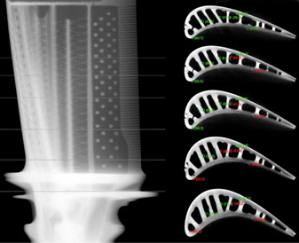
X-ray inspection of turbine bladesX-rays enable us to see the internal features of a variety of objects. Today, X-ray technologies are being applied in more and more areas across different industries. These technologies enable manufacturers and researchers to investigate the internal structures of objects without damaging samples. X-ray instruments are indispensible in designing, developing, manufacturing and inspecting airplane, automotive, electronic, and injection-molded(1) components and other items that are crucial to modern society.
Nikon X-ray instruments are used to inspect electronic products such as the wire bonding(2) and ball grid arrays (BGAs)(3) of semiconductor devices. Nikon also offers X-ray computed tomography (CT) inspection for industrial components such as jet engine turbine blades, castings, and injection-molded products.
Nikon’s X-ray inspection instruments are industrial-use X-ray CT inspection devices that take thousands of images and use them to formulate 3D internal structures, enabling optimum evaluation of the subject under inspection.
3D images created by Nikon’s X-ray CT inspection instruments have been employed in diverse applications, such as identifying voids(4) in BGAs or faulty electrical contacts in electronics components, identifying internal defects in castings, measuring complicated shapes that are impossible to measure without a 3D measuring device, and judging quality by comparing 3D data with computer-aided design data. For such fine measurements, the original images must be precise — and Nikon produces super-defined 3D images for every sample, even those composed of different materials.

XT H 450 LC X-ray CT inspection instrumentThe core technology of Nikon’s XT H 450 LC X-ray CT inspection instrument, the 450kV micro-focus source, is unique to Nikon. This system is indispensible for inspecting airplane engines’ turbine blades with nickel as their main component. The presence of nickel makes it difficult to inspect components with other, more conventional tools. Nikon’s XT H 450 LC X-ray CT inspection instrument allows for easier creation of 3D images of turbine blades, eliminating imaging concerns.
Nikon’s X-ray CT inspection system is used in a wide range of industrial fields. It is yet another example of the way Nikon promotes and enhances safety and security in diverse sectors.
- (1)A method of creating resin products or components by dissolving material using heat, filling it into castings using high pressure, then cooling and hardening it.
- (2)A method of connecting the electrodes of semiconductor chips with lead frames or conductors on a substrate via thin wires.
- (3)Ball grid arrays of electrodes on a substrate.
- (4)Empty spaces that are defects in a completed part.
- Products & Support ― Instruments Products
Take a look at Nikon’s wide array of instruments ― microscopes, measuring instruments, semiconductor inspection equipment, X-ray CT inspection systems, etc.
- 1. X-rays Reveal the Mysteries of Cultural Treasures
- 2. What Can X-rays Tell Us about the Universe?
- 3. X-rays Encounter the Infinitesimal World of Atoms